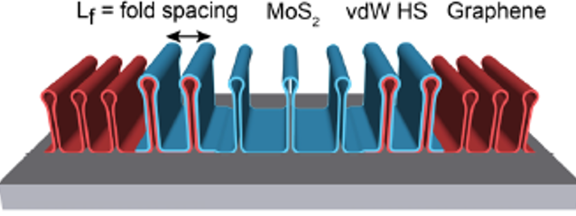
Researchers at the University of Illinois have developed ultra-flexible heterostructures made from 2D layers of van der Waals bonded materials. The heterostructures retain...
Researchers at the University of Illinois have developed ultra-flexible heterostructures made from 2D layers of van der Waals bonded materials. The heterostructures retain the optoelectronic properties of their constituent layers, but offer tunable mechanical properties which can include flexibility rivaling that of lipid bilayers. Applications for this technology include MEMS devices and flexible, stretchable, and conformal circuitry, including reconfigurable 2D devices and folded/curved/crumpled nanostructures.
Researchers from the University of Illinois have developed a platform for stretchable + flexible optoelectronics that offer consistent performance in stretched vs. non-...
Researchers from the University of Illinois have developed a platform for stretchable + flexible optoelectronics that offer consistent performance in stretched vs. non-stretched mode. The platform, which features stacked layers of two-dimensional materials that are crumpled or wrinkled, can enable new designs and manufacturing methodologies for devices that offer both toughness and malleability at scales as small as nanometers.
Since the 1960s, consumers, investors, and businesses have been able to rely on rapid advancement in semiconductor technologies according to Moore's Law, which states that...
Since the 1960s, consumers, investors, and businesses have been able to rely on rapid advancement in semiconductor technologies according to Moore's Law, which states that the number of components per semiconductor chip will roughly double every two years with minimal cost increase. For decades, semiconductor manufacturers were able to meet this expectation--and accommodate the huge increase in computing demand--by adopting designs, manufacturing methods, and other technologies that enabled smaller and smaller transistors (the basic building block of semiconductor chips). Continued increases in computing power and performance cannot be achieved in the same way, as today's transistors are so small that downsizing further would compromise the very physics of their operation. The industry has instead pursued increased transistor density by expanding beyond flat, two-dimensional transistor arrays to three-dimensional structures; first via FinFETs in the 2010s and now via even higher-aspect ratio gate-all-around (GAA) technologies.
Researchers have developed a suite of gate-all-around (GAA) devices to enable high and/or linear performance in a range of electronic applications. One asset encompasses a field effect transistor (FET) featuring between 2 and 20 vertically separated channels with some heterogeneity. The 3D high electron mobility transistor (HEMT) architecture utilizes ultra-wide bandgap (UWBG) materials and can be used for high-power, high-frequency applications. HEMTs can confer an order of magnitude higher performance than wide bandgap (WBG) devices, including simultaneously achieving 10x higher power density while operating at frequencies as high as 120 GHz.
Capturing polarized and visible light simultaneously is usually achieved by either rotating filters that reduce frame rate and need a static image or using an array of...
Capturing polarized and visible light simultaneously is usually achieved by either rotating filters that reduce frame rate and need a static image or using an array of sensors that must be aligned and can be bulkily and expensive. These issues are solved by Dr. Viktor Gruev's invention of a single chip that can detect both kinds of light simultaneously with high resolution and in real time. This sensor can detect 12 bands of visible light and 3 bands of polarized light. Because data is gathered in real time and does not require rotating filters, this sensor has applications in military surveillance, particularly in hazy conditions such as fog or underwater where polarized imaging can reduce background scattering information. Additionally, this sensor can be used in image-guided surgery, such as tumor removal used in combination with injected dyes that bind to cancerous cells that respond to different kinds of light.
Researchers at the University of Illinois have developed improvements to their innovative photonic integrated circuit (PIC) design, which features three-dimensional...
Researchers at the University of Illinois have developed improvements to their innovative photonic integrated circuit (PIC) design, which features three-dimensional subsurface networks of optical components (UIUC ref. no. 2017-212). The paradigm, called "volumetric photonic integrated circuits" (VPIC), addresses the bottleneck of large surface area requirements faced by conventional PICs by embedding the networks vertically within a semiconductor (e.g., porous silicon) material.
The present improvements include a variety of new subsurface components which exhibit low loss and high total efficiency competitive with silicon photonics. Components include high Q microrings; lenses and waveguides for efficient coupling; Mach Zehnder interferometers; loop mirrors; and distributed Bragg reflectors.
University of Illinois Urbana-Champaign researchers Songbin Gong, Ruochen Lu, Yansong Yang, and Steffen Link have fabricated an acoustic filter that functions with high...
University of Illinois Urbana-Champaign researchers Songbin Gong, Ruochen Lu, Yansong Yang, and Steffen Link have fabricated an acoustic filter that functions with high fractional bandwidth and low signal loss at gigahertz frequencies necessary for emerging 5G new radio technologies.
The acoustic filter is suitable for 5G mobile devices (e.g. smart phones), which will employ wavebands of higher frequencies than 4G technology. The device maintains small proportions without the fabrication challenges seen from scaling existing acoustic filter components present in 4G devices.
The filter employs a double layer of thin-film lithium niobate, a piezoelectric material, which serves to convert mechanical energy (radio waves) to electronic signals in 5G devices with better performance in the 3-6 GHz range than existing technologies.