
Processes
| Latest Innovations |
|---|
|
|
|
|
|
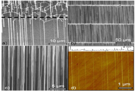
Carbon Nanotube Portfolio for Manufacturing ApplicationsThis portfolio includes carbon nanotube growth and processing methods relevant to nanotube manufacturing.... This portfolio includes carbon nanotube growth and processing methods relevant to nanotube manufacturing. Patterned Catalyst Techniques for Aligned Single-walled Carbon Nanotube GrowthSingle-walled carbon nanotubes (SWNTs) feature exceptional electric properties (conductivity and semi-conductivity) that make them attractive for nano-electronics, optics, material applications and more. This SWNT growth technology yields a dense structure without degraded alignment by eliminating undesired interactions between the SWNT and catalysts on the growth surface. More specifically, a patterned catalyst is used to provide a template to direct SWNT growth, resulting in perfectly aligned high coverage SWNTS. Benefits
Applications
Medium Scale Carbon Nanotube Thin Film Integrated Circuits on Flexible Plastic SubstratesThis technology improves the performance and consistency of integrated circuits featuring semi-conductive carbon nanotube (CNT) transistors. Specifically, metallic conductive pathways in random nanotube networks are reduced using a medium scale carbon nanotube thin film. This process reduces these pathways by cutting fine lines into the carbon nanotube network while preserving its semiconducting properties. Benefits
Applications
Using Nanoscale Thermocapillary Flows to Create Arrays of Purely Semiconducting Single-Walled Carbon NanotubesThis carbon nanotube (CNT) purification technology facilitates scalable, damage-free separation of arrayed metallic and semi-conductive CNTs. Resulting CNT arrays may be large and feature high Ion/Ioff ratios, allowing for less power loss while powered off, faster switching times, and overall lower operating voltage. The invention improves CNT array quality by creating a temperature gradient to release metallic CNTs from the array matrix. Benefits
|
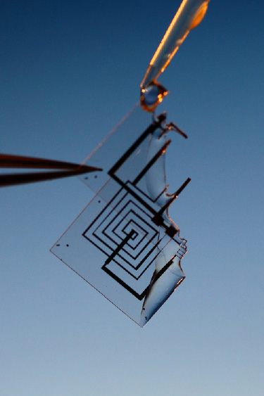
Suite of Bioresorbable and Transient Electronics
Transient electronic devices belong to a set of technologies, whereby traditional analog electronic circuits and components have been made in new ways. These new electronics exist on a much smaller scale and made of bioinert or biocompatible materials. They are flexible and transient. Transient and bioresorbable technologies are a class of device that have the ability to physically disappear at a programmed rate. Inventions within this suite includedevices and processes with applications rangingfrom medicine to construction, and from defense/securityto indoor/outdoor sensors. These technologies are appropriate for applications where device placement can be costly, invasive, or inconvenient to retrieve. Features
Benefits Electronics can now be implanted on surfaces with non-planar contact patches and non-invasive integration on soft, curvilinear surfaces of biological tissues and organs. Application Areas Remaking electronics with these capabilities permits for a plethora of new applications, in medicine, environmental research, biological enhancement, digital financial transactions and traceless surveillance.
|
|
 Bio-compatible