Heterogeneous Chip Integration of III-Nitride-based Materials for Optoelectronic Device Arrays in the Visible and Ultraviolet [1]
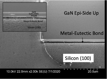
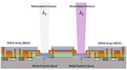
Professor Dallesassee and coworkers from the University of Illinois has developed a method for the heterogeneous integration of III-Nitride materials on various non-native substrates. This method uses a carrier wafer for the fabrication of the III-Nitride devices, which are then transferred to a host wafer and eutectically bonded. The method takes advantage of current tooling and allows for the fabrication of optoelectronic devices embedded into a CMOS platform for full electronic controls on a common substrate, such as silicon. These technique overcomes many of the limitations currently associated with the integration of III-Nitride materials such as their sub-par thermal performance, and the high costs associated with the handling and alignment of the III-Nitride devices onto the substrate.